
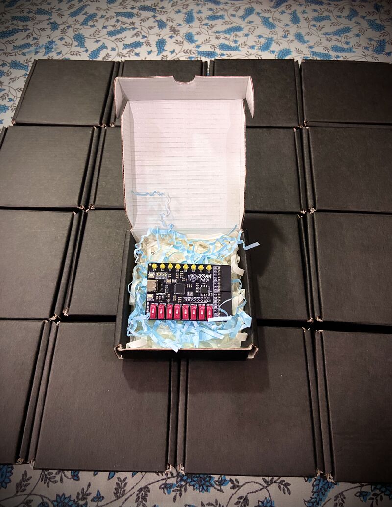
Soan Papdi FPGA!
*No MCU. Pure FPGA!
Soan Papdi is a learning-focused FPGA board built around the Lattice iCE40UP5K, making FPGA development simple and approachable for learners.
The design is intentional - Just
the FPGA, Flash memory, a USB-C port for power and loading circuits, and Basics Input/Output.This is THE board if you wanted to dip yours toes and try Digital Design!
4 Steps - Zero to Hero!
for kids and adults alike
Technical Specifications
For beginners and experts alike!
- Lattice iCE40UP5K FPGA with 5,280 LUTs.
- 128 Mbit onboard Flash memory.
- On-chip PLL. Internal 10 kHz and 48 MHz Oscillators.
- 2 × SPI and 2 × I²C Hard IPs
- 8 DSP multiplier blocks.
- Capable of hosting RISC-V soft-core CPUs.
- USB-C fully controlled by FPGA (no ext. MCU).
- Programmable via preloaded DFU bootloader.
- 3.0 mm LEDs (through-hole)
- 4 × SMD LEDs
- 8 x DIP switches
- 2 push buttons (Programming & Reset)
- 10 x I/O pins for ext. sensors & peripherals.
Minimal Design
less is more

Free Lectures
Lectures to guide you on how to use the board
This is a ever growing resource
the backstory
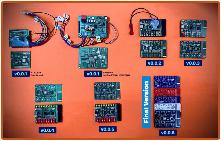
Soan Papdi is deliberate and very intentional
Soan Papdi board is designed to be easy to use, be simple in design and not limit the learner.
the team
a collaboration between Pyjama Cafe and DIY with Hardik
An embedded product engineer who designs PCBs, writes firmware, and enjoys turning ideas into complete, working hardware products from first schematic to final blink.
Engineer by day, Maker by night - playing with electronics since the age of 9. From childhood, I’ve loved tearing things apart, rebuilding them, and learning through hands-on experimentation and how-to videos.

Electrical Engineer holding a Master’s degree in Embedded Systems, with a proven track record at industry giants. At Intel, contributed expertise to Navigation Firmware, Bluetooth Driver development, and RF validation software.
Currently thriving as an Embedded Software Engineer at Google, drove innovation in Firmware development for the Power Management Sub-system on Tensor SoCs (Pixel Phones) and presently advancing system software for the Pixel Watch.
Proposal of Soan Papdi was made by Piyush, the idea was brought to life by Hardik.
Made with Love and Care, in India ❤️